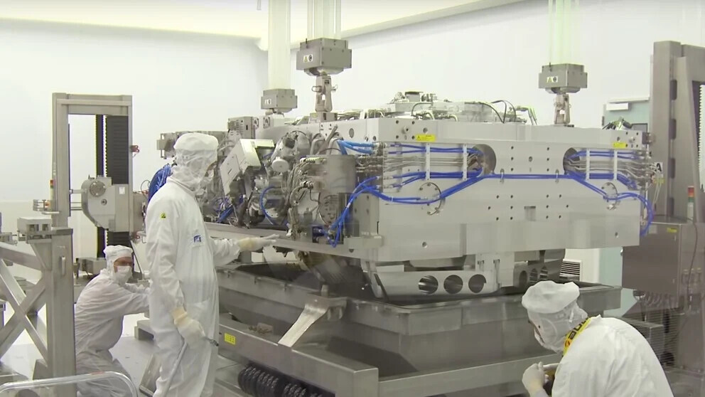
Its ASMLs most high-end tool to date.
Now, imec says that the use of the technology has already yielded impressive results.
This essentially translates to super small and densely-packed circuits that can deliver more powerful and efficient chips.
40% off TNW Conference!
Exposure is the process when light is used to transfer a pattern onto a semiconductor wafer.
The patterns for the logic chips were also printed in a single exposure.

Van den hove also pointed out that these demonstrations will accelerate the introduction of these tools into manufacturing.
Story byIoanna Lykiardopoulou
Ioanna is a writer at TNW.
With a background in the humanities, she has a soft spot for social impact-enabling technologies.
